


Abstract
Hot Trends in the Semiconductor Industry – The high-performance computing (HPC) market is rapidly growing globally, further driving the development of widespread applications such as 5G, cloud data centers, artificial intelligence, mobile computing, and self-driving cars. As advanced processes continue to be developed, market demands for high computing power, low latency, and low power consumption in design products are driving the evolution of high-speed access interface applications, specifications, and advanced processes. The investment in specialized division of labor and EDA tools by Foundries have significantly increased, making the demand for advanced process high-speed interface IP integration hard-core implementation increasingly high.
Diversified high-speed interface application specifications and advanced processes
As the performance of electronic device processor chips increases, the demands for high-speed data transfer are further increased. There are a variety of high-speed access and visual surveillance interfaces, such as SATA, USB, PCIe, MIPI, etc. Just like various modes of transportation, chip designers often target a few types of transmission technology specifications based on their own product applications. Therefore, the only way to stay ahead of the curve is to continue to refine the technology as it changes from one generation to the next.
In today’s massive real-time high-speed computing, there is an ultimate pursuit of low latency and low power consumption, which drives the advancement of advanced chip manufacturing processes such as FinFET. In the process of implementing advanced processes in chips, apart from the training of professional talents, the purchase of different EDA tools, packaging and testing are all necessary investments, which will lead to a significant increase in overall production costs and increase the difficulties and risks for chip manufacturers to enter the high-speed computing market.
In the chip design process, from the specifications of the product itself, to the verification of various IP designs, and even to the integration and implementation of the entire chip, it is necessary to comply with the market’s key criterion – Time to Market. Facing huge schedule pressures and unfamiliarity with the high-speed interface expertise, it is undoubtedly a challenge for every engineer and company to understand the different specifications of high-speed transmission access interfaces in a short period of time, and to gradually complete the verification from IP level, Sub-system level to Whole chip level, and win in the fiercely competitive market while taking on risks.
Highly Integrated Specialized Division of Labor
In SoC chips, many high-speed transmission access interfaces include the physical layer (PHY) and the control processor (Controller). Different high-speed interface specifications represent different areas of expertise. In the case of unfamiliarity with the high-speed transmission interface know-how, the integration and implementation of a fast and complete verification in a short period of time can be highly risky.
M31 has completed the design development and verification of high-speed interface IP for PCIe, MIPI and USB on 40nm, 28nm, 22nm and FinFET processes, alone with verification methods of different interfaces control processors and sub-systems (Figure 1) to achieve one-stop service for high-speed interface integration (Figure 2). This service helps customers to integrate sub-systems into SoC quickly and easily through the AMBA architecture, reducing risks and allowing customers to focus on differentiated chip design and system-level integration, making their IC products more competitive in terms of performance and cost-effectiveness.
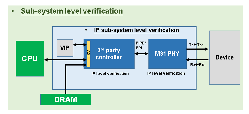
Figure 1. Sub-system level verification

Figure 2. IP Integration Service
For SoC designers, IP is seen as a black box. To achieve the best results with the least amount of effort, it is essential to provide a portfolio of design kits that will integrate the standard system interfaces.
M31 provides a complete design kit package, including a behavior model, controller body, integrated IP simulation environment, constraint file, and EDA software (Sign-off, Data-in) quality analysis reports to further protect customers from incompatibility issues with the original SoC.
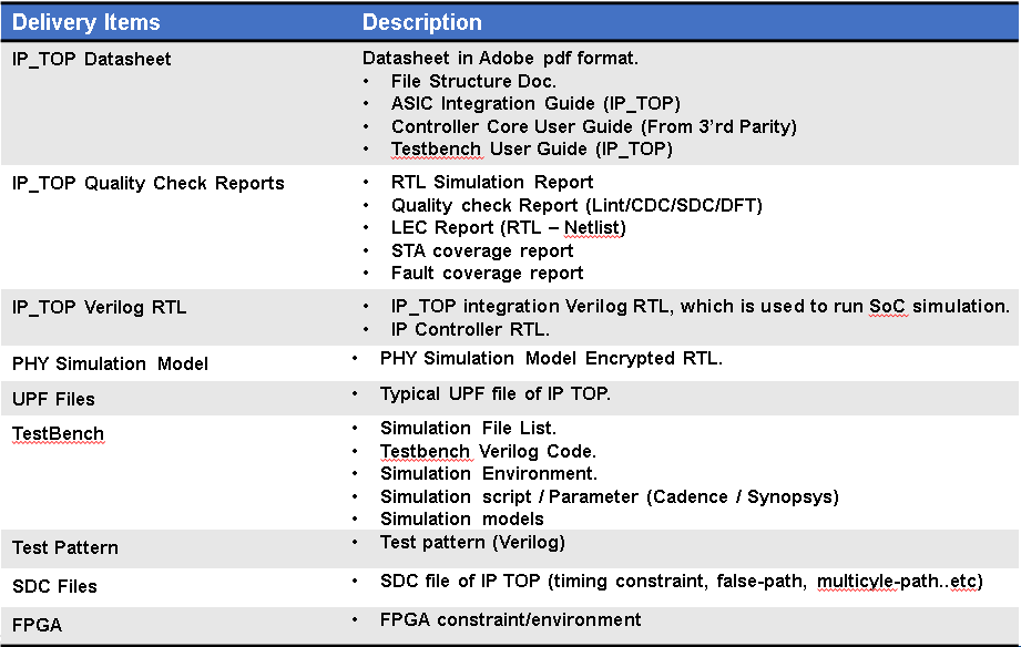
Table 1. Design Kit Set
M31 High Speed Interface IP Integration One-Stop Service
With the rapid evolution of manufacturing processes, from traditional IDM companies leading chip development, to the diverse application areas of SoCs and professional IP specialization, the process and risk management of chip design are always being challenged. In addition to continuously developing the latest generation of IP products for advanced processes, M31 further provides integrated hardcore implementation services for customers, allowing designers to reduce risks and achieve maximum benefits in the market of high-speed computing and access interface applications that demand both performance and power consumption, and to seize the market niche.