


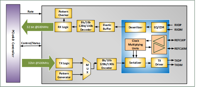
M31 PCIe 4.0 PHY IP provides high-performance, multi-lane capability and low power architecture for high-bandwidth applications. The PCIe 4.0 IP supports a complete range of PCIe 4.0 Base applications and is compliant with the PIPE 4.4.1 specification. The IP integrates high-speed mixed signal circuits to support 16Gbps PCIe 4.0 traffic and is backward compatible with 8.0Gbps PCIe 3.1, 5.0Gbps PCIe 2.1 and 2.5Gbps PCIe 1.1 data rates. With the support of TX and RX equalization techniques, the PCIe 4.0 IP is designed to meet the requirements of different channel conditions.
- IP Product Lists
- Features
- Fully compliant with PCI Express Base 4.0, PCI Express Base 3.1, PCI Express Base 2.1 and PCI Express Base 1.1 electrical specifications
- Compliant with PIPE4.4.1 (PCIe) specification
- Supports all power saving modes (P0, P0s, P1, P2) defined in PIPE4.4.1 specification
- Supports L1 PM Substates with CLKREQ#
- Supports L1 Clock Power Management (CPM) with CLKREQ#
- Supports Separate Refclk Independent SSC (SRIS) architecture
- Accessible register controls allow user-specific optimization of critical parameters (e.g., TXPLL bandwidth, TX de-emphasis level, CDR bandwidth, and EQ strength)
- Supports robust BIST functions for mass production testing
- Dual-mode reference clock pad: Output 100-MHz clock reference clock for RC mode or receive 100-MHz clock for EP mode
- Can be configured up to multi-lane (x4, x8, x16) design with multiple instances
- Available in 12nm/16nm, 7nm, and 5nm processes