


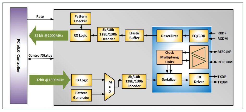
M31 PCIe 5.0 PHY IP provides high-performance, multi-lane capability and low power architecture for high-bandwidth applications. The PCIe 5.0 IP supports a complete range of PCIe 5.0 Base applications and is compliant with the PIPE 5.2 specification. The IP integrates high-speed mixed signal circuits to support 32Gbps PCIe 5.0 traffic and is backward compatible with 16 Gbps PCIe 4.0, 8.0Gbps PCIe 3.1, 5.0Gbps PCIe 2.1 and 2.5Gbps PCIe 1.1 data rates. With the support of TX and RX equalization techniques, the PCIe 5.0 IP is designed to meet the requirements of different channel conditions.
- IP Product Lists
- Features
- Fully compliant with PCI Express Base 5.0 electrical specification
- Compliant with PIPE5.2 (PCIe) specification
- Supports all power saving modes (P0, P0s, P1, P2) defined in the PIPE5.2 specification
- Supports L1 PM Substates with CLKREQ#
- Supports L1 Clock Power Management (CPM) with CLKREQ#
- Supports Separate Refclk Independent SSC (SRIS) architecture
- Accessible register controls allow user-specific optimization of critical parameters (e.g., TXPLL bandwidth, TX de-emphasis level, CDR bandwidth, and EQ strength)
- Supports robust BIST functions for mass production testing
- Programmable differential reference clock pad that can receive or transmit 100MHz reference clock
- Built-in PLL for receiving 25MHz crystal clock and generating 100MHz reference clock for RC applications
- Built-in LDO for analog core power generation, providing easier IC integration and lower BOM cost for SSD applications
- Macro-based cells that can be combined into bifurcation applications
